Computer storage may not get more miniature-sized than what has, in principle, been reached, says S.Ananthanarayanan.
The space taken for electronic data storage has shrunk as fast as computing capacity has increased. While computing speed is now at billions of a second, the size of the components in microcircuits has dropped from microns to as low as 45 nano meters, or thousandths of a micron. The first hard disks were marvels that stored 260 MB and now they store in TB, or approaching a million times more than what they used to. Keeping up the pace of miniaturization, however, has become challenging, as the dimensions of the storage components are fast approaching the physical limits to how small things can get and still function.
But an achievement in miniaturisation, which has just been reported, may well be the end of the line. F. E. Kalff, M. P. Rebergen, E. Fahrenfort, J. Girovsky, R. Toskovic, J. L. Lado, J. Fernández-Rossier and A. F. Otte, from the Kavli Institute of Nanoscience, Delft, the Netherlands, the International Iberian Nanotechnology Laboratory in Portugal and the Universidad de Alicante in Spain, report in the journal, Nature Nanotechnology, their success in storing a reasonable quantity of data in a format reduced to the size of individual atoms!
The best data storage used so far works with the help of magnetic regions which are just below a micrometer in size and along the length of a film of magnetic material. Each of these regions can be magnetised in one of two directions, and the sequence of regions can represent the digits, -‘0’ or ‘1’, so that data can be stored in binary form. Each of these magnetized regions, in turn, consists of some hundreds of crystal grains, and each grain, of course, consists of millions of atoms. A good part of the progress and improvements in storage technology has been to use smaller regions for each ‘bit’, or the option of ‘0’ or ‘1’, of information, in such a way that one region does not disturb the other and also that it is practical for each region to be ‘written’ and ‘read’.
A great advance, through the manipulation of individual atoms, either for fabrication of components or for recording data, became a possibility with the development of the Scanning Tunneling Microscope (STM), which is used to detect matter at the level of atoms. The actual microscope consists of a metallic tip, a needle, which has been sharpened so that its tip is just a single atom. Now, the free electron cloud associated with atoms of a metal, which the microscope is to study, extends just beyond the metallic surface. If the tip of the STM is brought really close to the metal surface, electrical forces start acting between the tip of the needle and the surface.
While just in this position of extreme proximity, if a small electric potential is applied to the metallic tip, an electron could move from the tip to the metal surface, ‘tunneling’ through the repulsive electron cloud, and an electric current would flow. As the current rises sharply if the tip comes even an atomic diameter closer, the current becomes a measure of the evenness of the surface as the tip scans the surface.
STM in action
It is the same technology that the authors of the paper have used to manipulate atoms to record data. With only this difference, that in place of measuring a spurt in the current, they supplied the tip of the STM with a small voltage when they wished to nudge a chlorine atom in a honeycomb of copper atoms from one slot to the next.
The first time the STM was used to move atoms was in 1990 when Don M Eigler and E K Schweizer stationed xenon atoms on a nickel surface in pattern that spelt the letters, “IBM”. Ever since then, the Nature Nanotechnology authors say, atomic arrangements have been assembled by in this way by lateral positioning of atoms and molecules that have been deposited on a flat metal surface.
This method, they say, is good with up to some hundreds of components, but because there is no framework on the metal surface, creating a complex and close-set patterns is not feasible. And further, the procedure needs to be carried out at exceedingly low temperatures. Instead, the new procedure they have developed allows accurate placing of chlorine atoms in a regular and extended array and is possible at a more practical temperature.
The basis of the method is a raft of chlorine atoms which assemble themselves into a regular lattice on the surface structure of crystalline copper. This arrangement of chlorine atoms, according to the spacing of the copper atoms, forms a large grid on which specific shapes can be drawn. There could also be vacant spaces, or vacancies between the chlorine atoms. And then, the lattice remains stable at comparatively higher temperatures, that is, as high as minus 196°C. This temperature can be maintained by using liquid nitrogen, which is easier than lower temperatures which need liquid helium. But the best feature is that the position of the chlorine atoms can be readily changed with a nudge using the Scanning Tunneling Microscope.
These features, the authors say, allow for a very large pattern of occupied and vacant spaces in the grid to be built up with great reliability and speed. Representing data according to the pattern of the grid would hence allow data to be written onto the copper surface and also to be deleted or edited as desired. Comparably large atomic-scale data storage has been demonstrated using individual silicon atoms placed on a silicon-gold surface, the authors say. But this arrangement, unlike the present one, cannot be modified at will and needs to be completely regenerated to change even one bit, they say.
The method now developed is to fix a point on the copper base as a ‘marker’ and distribute the chlorine atoms, or vacancies in different blocks. The positions were ranged in rows of eight pairs, each pair consisting of either a chlorine atom or a vacancy, with separators all round each pair. As each pair could be either ‘atom- vacancy’ or ‘vacancy-atom’, each pair could represent either ‘1’ or ‘0’ and the row of eight pairs would represent the eight bits that computers use to store an item of data.
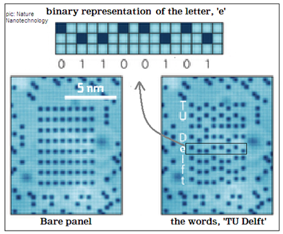
The researchers have succeeded in creating a panel of such rows to represent 1,016 characters, that is to say, the letters, punctuation and spaces, of a whole text passage, within a 96 x 126 nanometer chip. The passage, which can be readily read and re-written with an automatic procedure, is a whole KB, or 8,000 bits and the storage density works out to 502 terabits per square inch, which is hundreds of times more dense than the best hard disks.
The technology is still far from ready for the industry, as it has been tested only in the laboratory and does need a temperature of nearly minus 200°C, A new paradigm of data storage, however, has been proved in principle and shows the way to very high storage density, which would be useful for archiving of massive data and also for high capacity, miniature devices
------------------------------------------------------------------------------------------
Do respond to : response@simplescience.in
